[Automatic translation by Google]
Please provide your feedback about the website at feedback@apc.iisc.ernet.in
Dean EECS’s note: Padma Bhushan V Rajaraman, IISc Distinguished Alumnus (ECE), Retired Professor, Supercomputer Education & Research Centre and Computer Science and Automation, Indian Institute of Science, discusses his move from IIT Kanpur to IISc and the start of the CAD Lab.
Prologue
I joined the Indian Institute of Science, Bangalore (IISc), on the invitation of Prof. Satish Dhawan who was the then Director of the Institute. I was to join in 1981 but was delayed as the Indian Institute of Technology, Kanpur, was unwilling to relieve me. After some persuasion, IIT/Kanpur allowed me to accept the Professorship offered by IISc on deputation from IIT/Kanpur for 2 years starting 1982 with the option of returning to IIT/ Kanpur. When I joined in June 1982 Prof. Satish Dhawan had retired and Prof. S. Ramaseshan had taken over as the new Director. There was hardly any activity in the area of Computer Aided Design of Electronic Systems at the IISc. I also quickly found out that to build a research group, get equipment, travel to conferences etc., it was essential to obtain funding from outside (normally the Central Government) as the Institute’s budget was meagre.
As soon as I joined the Institute, the Director Prof. S. Ramaseshan appointed me as the Chairman of the Computer Centre and Professor in the School of Automation (which was later renamed the Department of Computer Science and Automation).
Proposal to set up a Centre for Computer Aided Design (CAD)
I was aware that the Department of Electronics (DOE) of the Government of India (GOI) was planning to allocate funds for supporting a centre for Computer Aided Design (CAD) of Electronic Systems. DOE had also sent a proposal to the United Nations Development Programme’s (UNDP), India office to support this activity. I sent a proposal to the DOE to set up a Centre for Computer Aided Design of Electronic Systems at IISc requesting grants for a building, equipment, and scientific staff. The main objectives of the Computer Aided Design Centre for Electronic Systems as given in the proposal were:
I insisted that we needed a building as the Computer Centre at IISc had little extra space and that the Institute did not have funds to allocate for a new building. The original proposal requested a grant of Rs.90 lakhs and USD 200,000 (from UNDP) for constructing a building, buying computers and software, training engineers overseas, recruiting scientific officers and other staff, and conducting workshops. I was called for a discussion with the officials of DOE and a meeting was held in early September 1982. An official of DOE and a consultant to UNDP visited the Institute in late September 1982 to assess the capability of the Institute to establish such a centre. In 1983 DOE scheduled a meeting in Delhi which was also attended by Prof. S. Ramaseshan (the then Director of the Institute) to finalise the amount and mode of funding and a Memorandum of Understanding (MOU) which was to be signed between the Institute and the DOE on the general administrative structure of the Centre and how it should operate as a part of the Institute. It was agreed that the Computer Aided Design Centre was to be a separate entity and not part of the Computer Centre or any other existing department of the Institute. DOE was concerned about the continuity of the research programme in this area at the Institute as the funding was substantial. Normally project funding does not include money for buildings. However, I again reiterated that the Institute had a space crunch and the activity cannot progress unless building fund was granted. The MOU included a section on locating the building in the Institute and future maintenance of the infrastructure. After protracted negotiations a formal sanction for setting up a CAD Centre was given by DOE in March 1984 along with an initial grant of Rs.16.25 lakhs. A grant of Rs.18.5 lakhs was promised for the financial year 1984-85. The Institute as per the MOU with DOE created a CAD Centre and I was named the chairman.
Once the sanction came in March 1984, I got an architectural design for the building. The building was to be built in the open plot opposite the (then) School of Automation. When this plan was shown to the Director, he said that there was a problem regarding the location as the Department of Metallurgy wanted that area for future expansion. The Director Prof. S. Ramaseshan opined that the area on the north side of the existing Computer Centre building was empty. He was also of the opinion that it was time to change the culture of each centre/department in the Institute having a separate building. At about the same time DOE had granted funds for a building to CEDT (now called DESE) and also for a Microprocessor Applications Laboratory (MAL now closed). Dr. Ramaseshan decided that there will be only one building built consolidating the grants given to the three activities. The space in the building was to be shared proportional to the amounts each one contributed towards the building. The contribution of Computer Aided Design Centre was Rs.25 lakhs entitling it to get a plinth area of around 10000 Sq.ft in the building. I as the Chairman of the CAD Centre agreed to cooperate with the other stake holders (namely, CEDT and MAL). CEDT was already well established with funding from the Swiss Government and DOE and their building grant was substantially higher than that of CAD Centre. Thus, our area was about 1/3 of the total area of the original building which was built.
Stup Consultants (an architectural and structural engineering company) was engaged as the architects and it planned the building with a committee of all the stake holders. (Prof. N. J. Rao, Mr. Andre Pitet of CEDT, myself, and Dr. N. Balakrishnan representing MAL). Mr.Pitet and Prof. N.J. Rao spent a lot of time in laying out the location of rooms, sizes of rooms, laboratories etc., for CEDT and I did the same for the CAD Centre. We had also agreed that later we will cooperate in our respective research activities. (I was at that time a co-opted member of the CEDT steering group). When the building contractors dug the ground for laying the foundation it was found that it was a filled area and water table was quite high. Water had to be pumped out and the foundation design had to be modified in the changed circumstances. The building construction started in late 1984 and was ready for occupation in 1988.
Initial Activities of CAD Centre
Meanwhile as per the MOU with DOE an advisory committee for the CAD Centre with the Director of the Institute as Chairman was constituted The advisory committee’s Chairman was Prof. C. N. R. Rao (Prof. S. Ramaseshan retired in July 1984 and Prof. C.N.R. Rao took over as the new Director in August 1984) , a representative of DOE, 3 representatives from the Electronics Industry (we had representatives of Bharat Electronics Ltd., Bangalore, Indian Telephone Industries Ltd., Bangalore, and Semiconductor Complex, Mohali), two experts from outside the Institute and me as a member secretary. As the advisory committee was to meet only once a year, a Centre Programme Committee with me as Chairman and Professors from ECE Dept., CEDT, EE Department, and the School of Automation was formed to steer the activities of the Centre.
The activities of CAD Centre did not wait for the building to be ready. Even though the computer centre of which I was the chairman was quite cramped, we readjusted desk spaces and laboratory area to accommodate the scientific staff we had started recruiting for the centre. I requested S.K. Nandy who was a scientific officer in the Computer Centre and had registered as a M.Sc. (Engineering) student (working in the area of CAD electronics) to get associated with the activities of CAD centre in addition to his duties in the computer centre and he readily agreed. His association with the CAD centre proved invaluable in the development of the centre. In addition, three scientific officers were initially recruited for the centre. They were allowed to register for their doctoral degrees in the Institute as that was the only method which allowed the centre to recruit high caliber scientific officers who already had a Master’s degree in electronics. I went to U.S.A on UNDP assignment in September 1984 to explore Universities which would accept the scientists from our CAD Centre for training for about 4 to 6 months. I visited MIT, University of California, Berkeley, State University of New York at Stony Brook, Concordia University and the University of Waterloo in Canada to explore training opportunities and also to identify professors who would visit IISc for 4 to 8 weeks to give courses in VLSI design using software which would be available from the Universities in this area. One of the problems faced by India during the period 1984 – 90 was denial of export license for what was considered high technology (Hi Tech) by the United States government and some of its allies. Hi Tech included computers and commercially available software in the area of VLSI design and even software to design multilayer Printed Circuit Boards (PCB). One of the aims of the CAD centre was to establish collaboration with Universities abroad and get prototype software developed by the Universities, which we thought would not require export clearance. The plan was to install the software on our computers, train engineers in using and understanding the software which they would improve by adding modules. I felt that after this learning experience our engineers would be able to develop software in CAD to suit the needs of the electronics/computer industries in India. University of California, Berkeley, was well known in developing VLSI design software and I was keen on establishing a link with it. However, the Professors at Berkeley were reluctant to commit as they were receiving funding from the Department of Defence, U.S.A. State University of New York at Stony Brook, though not as well-known as the University of California at Berkeley, had Professors working in CAD area and Prof. David Smith whom I knew earlier was willing to commit his laboratory for long term collaboration. A well-known Professor at MIT was also willing to come and give a course on VLSI design with the software developed by his team at MIT.
Meanwhile DOE formed a committee with UNDP experts to suggest appropriate computers for the CAD Centres set up with DOE and UNDP funding. There were four CAD Centres supported by DOE. Besides the one at IISc, Centres were at IIT/Kanpur in mechanical and structural engineering, at IIT/Bombay in chemical engineering, and at Jadavpur University in heavy engineering. DEC VAX11/780 was recommended for all the four centres by the committee and orders were placed. However, the centres could not buy VAX11/780 due to denial of export license by the U.S. government. It was decided that each centre would look for alternatives based on their own evaluation of systems appropriate for their software development.
Equipment Purchase
An equipment procurement committee was formed with me as Chairman and with Prof. B.S. Sonde, Prof. I.G. Sarma, Prof. N.J. Rao, and Prof. L.M. Patnaik as members. The committee was assisted by Mr. S.K. Nandy. The committee after exploring the various options and keeping in view the export clearance problems recommended procurement of the following computers for the CAD Centre.
These systems were installed by late 1987. In 1988 one HP 9000/550 dual processor system was acquired when the building was ready for installing this system. More systems were added and by 1989 the Centre had the following systems operational:
All the above systems were connected by a local area network.
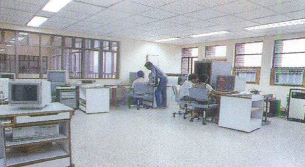
HP Systems and graphic stations in the CAD Centre
Training of Scientists of CAD Centre
One of the objectives of the CAD Centre was to train scientists in software development in CAD of electronic systems. A major component of UNDP assistance was for training and for inviting experts from abroad to conduct workshops in this area. Based on my earlier visit to explore training opportunities the following scientific officers were sent for training for periods shown against their respective names:
| S.K. Nandy | State University of New York at Stony Brook, U.S.A | Aug.85 – Feb.86 |
| D.K. Anvekar | State University of New York at Stony Brook, U.S.A | Jan.86 – Aug.86 |
| S. Sundaram | State University of New York at Stony Brook, U.S.A | Aug.86 – Feb. 87 |
| M.K. Srinivas | Concordia University, Canada | Nov.87 –May 88 |
When they returned, they were in a position to develop software in the CAD area. S.K. Nandy, S. Sundaram, and M.K. Srinivas worked full time in the CAD Centre whereas D.K. Anvekar was a scientific officer in ECE Department and was associated part time with CAD centre.
Expert Visitors
UNDP had allocated funds to invite professors from aboard to conduct workshops and guide our scientific staff in installing and using CAD software. Prof. David Smith of the State University of New York at Stony Brook who had provided training opportunities for our scientific staff and was an expert in the area readily agreed to spend 8 weeks (Jan 1988 to March 1988) at IISc. During my visit in Sept. – Oct 1984, I had also discussed the possibility of a visit by a professor who was leading the CAD activities at the Massachusetts Institute of Technology to conduct a workshop using the VLSI CAD software developed at MIT and leaving the software behind which would enable us to use it for conducting courses at IISc. He agreed and accordingly I requested UNDP to extend an invitation to him. He accepted the invitation. I corresponded with him stating our requirements. He said that he would be able to conduct the workshop with the software developed at MIT but will not be able to leave it behind due to export control regulations of the U.S. Government on CAD software. This was not acceptable as the main purpose of inviting experts was to have a continuing relationship in software development. I wrote to UNDP to withdraw the invitation to the professor from MIT. Meanwhile I started exploring the availability of other experts. When I had visited Stanford University, Prof. Thomas Kailath had mentioned that some good work was being done at the Technical University of Delft (TU, Delft) in the Netherlands by Prof. Patrick De Wilde’s group. A software for VLSI design called NELSIS. (Netherlands Large Scale Integrated Circuit Software) had been developed by Prof. Patrick De Wilde’s group at TU, Delft. I wrote to Prof. De Wilde enquiring whether he would be able to conduct a workshop on VLSI designs using NELSIS developed by his group and leave the source code behind for our group to use and possibly improve. Prof. De Wilde readily agreed and accordingly I requested UNDP to extend an invitation to him. He agreed to come in January 1988 for 4 weeks along with a colleague of his, Dr. T.G.R. Van Leuken. An invitation was extended to him also by UNDP. By 1988 we had already bought an HP system and NELSIS source code written in C language could be installed in it and used for conducting a workshop. A workshop was conducted from Jan.20 to 29, 1988 on LSI/VLSI design with lectures and laboratories conducted by Prof. David Smith, Prof. Patrick De Wilde, and Dr. T.G.R. Van Leuken. NELSIS software was used extensively in this course. This was the beginning of a long fruitful technical collaboration between the TU, Delft and the CAD Centre at IISc. Fortunately, there was no formal MOU and bureaucracy in our relationship which lasted from 1988 to 1998. Dr. T.G.R Van Leuken came again during August-September 1988 as a UNDP expert.
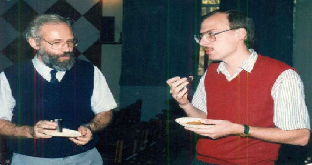
Prof. Patrick De Wilde and Dr. TGR Van Leuken during tea break of the workshop
CAD Centre Projects
There were several projects which were carried out by the scientific staff and students (registered for M.Tech degree in CSA and ECE Depts). At the peak of its activities CAD Centre had 4 scientific officers, 3 scientific assistants and around 30 Masters’ students working on several projects. The scientific officers who had long association with CAD centre were Dr. S.K. Nandy, Dr.S. Sundaram, Dr. M.K. Srinivas and Ms. Naga Venkataramana. Support staff consisted of Ms. A. Sarala Devi (office-in-charge) and Aswatha (Helper). Care was taken to choose projects which would be useful to industries in India, were of educational value, and could be implemented on the smaller configuration computers available in the CAD centre and the industries.
The projects were
By 1989-90 the following software systems were installed and were being used in the CAD Centre:
Workshops conducted by CAD centre
One of the aims of the CAD centre was to conduct hands-on workshops in the area of computer aided design of electronic systems. Besides short lectures on theory, the major part of the participants’ time was spent in using the tools developed by the centre staff and studying the source codes which were made available freely. The following workshops were conducted at the CAD centre:
From the above list it is clear that industries were the main participants in these workshops as envisaged when the CAD centre was established.

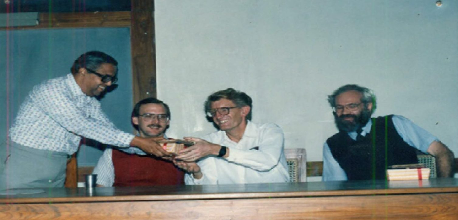
Prof. Rajaraman giving a memento to Prof.David Smith after his lectures in the workshop on VLSI Design. Also seen in the picture are (left to right) Dr. TGR Van Leukan and Prof. Patrick De Wilde.
Multiplier effect of NELSIS software
The availability of NELSIS source code was of immense value to the scientists in the centre who could delve deeper into it. It was improved further when Dr. T.G.R Van Leuken visited CAD centre again during Feb-March 1990. Meanwhile the CAD group at ITI Ltd., Bangalore was interested in porting NELSIS to their computer system. ITI had difficulty in importing VLSI design software. The integrated circuit design group at Defence Research and Development Organization (DRDO), Hyderabad, called Applied Numerical Analysis Research Group (ANURAG) was also interested in porting NELSIS to their computing system as it was designing an indigenous version of Intel 80386 and wanted VLSI design software. Prof.De Wilde had no objections to sharing the software as feedback from users would help us improve the software. We negotiated with ITI Ltd. and ANURAG regarding license fee and help in porting the software. NELSIS was licensed to ITI Ltd. and ANURAG on payment of Rs.10 lakhs each. It was decided that this fund of Rs.20 lakhs would be used primarily for TU Delft-IISc CAD Centre collaboration, namely, inviting professors from TU Delft and sending our scientists to work in TU Delft. As mentioned earlier the collaboration began in 1988 and continued for around 10 years. The money was not used for buying equipment; it was mainly used for exchanging visits and conducting workshops to enhance cooperation between research groups at TU,Delft and the CAD Centre.
The NELSIS funding was used to conduct the following workshops:
End of DOE CAD Centre project and follow up
The original project sponsored by DOE was for 5 years from 1984 to 1989. However, as the first grant money came only in March 1984 and we started work only in 1985, the project was extended to 1991. The total funding received from DOE and UNDP for this project was:
| (i) | Equipment | : US$ 22,350.00 |
| (ii) | Training of Scientists abroad | : US$ 65,800.00 |
| (iii) | Experts visits/consultancy | : US$ 80,300.00 |
| TOTAL | : US$ 168,450 |
As I foresaw the end of DOE funding for CAD Centre, I applied to the National Microelectronics Council (NMC) of DOE to fund VLSI design related projects so that the activities in this important area could be continued beyond 1991. A funding of Rs.59,76,000.00 was approved by NMC to sustain the activities of Centre till 1993. The projects funded by the NMC included:
Even though the MOU which DOE signed with IISc had envisaged IISc taking over the funding of the centre after the end of the project, the new administration was not very keen on this. After the reorganization of the Departments, Schools, Centres, and Laboratories of the Institute by the Director in 1991, the CAD Centre was named CAD Laboratory. The logic was that CAD Centre did not have sanction for faculty to be able to supervise M.Sc and Ph.D theses. Centres were allowed to award degrees whereas laboratories were primarily intended to work on projects. In 1992-93 we had 3 scientific officers who were on the permanent staff of the laboratory. The DOE funding was also coming to an end and I was due to retire in 1994. The Director decided in 1993 that CAD Laboratory would be merged with the Supercomputer Education and Research Centre and the scientific staff will be absorbed by SERC. However, it was decided that research in the CAD area would continue in the CAD Laboratory which would function in its own building with external funding. In 1994 there were three faculty members: Prof. V. Rajaraman, Prof. S.K. Nandy, and Prof. V. Viswanathan (who were on the rolls of SERC), 3 scientific officers (Dr. S. Sundaram, Dr. M.K. Srinivas and Ms. Naga Venkataramana) and 2 office staff (Ms. A. Sarala Devi and Aswatha). S.K. Nandy, S. Sundaram, and M.K. Srinivas obtained Ph.Ds. while working in the CAD Centre. Dr. S.K. Nandy did outstanding work independently in CAD and was designated Assistant Professor in 1989. After I retired in July 1994, Prof.S.K. Nandy led the group and was able to get funding from Philips Research Laboratory and ST Microelectronics Laboratory and was able to attract very good research students to continue the research activities of the CAD Laboratory.
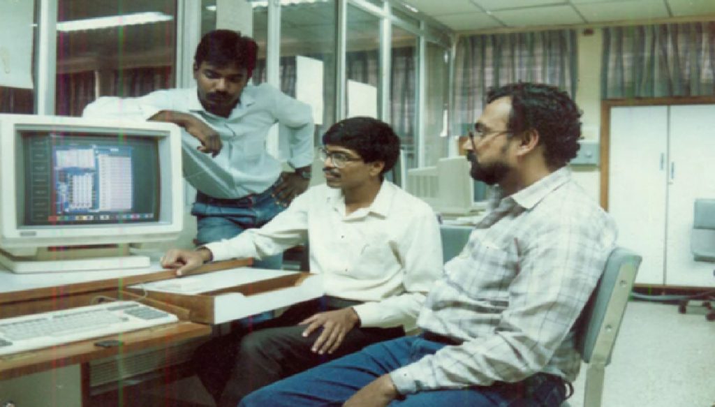
Prof. SK Nandy, Dr.Rajat Moona (who was in the KBCS group), and Ranjit an M.E. student discussing a Printed Circuit Board layout using a graphics terminal
Knowledge Based Computer Systems Development Project
While the CAD Centre was getting established, I sent a proposal to the DOE requesting that IISc be allowed to participate in the Knowledge Based Computer Systems Development (KBCS) project which was funded by the UNDP and the Govt. of India (DOE). My proposal was accepted by DOE. This project’s objectives were similar to the ongoing “Fifth Generation Computer Project” which was initiated in Japan in the early eighties. KBCS project was distributed across India in seven institutions. The objectives of the KBCS group at IISc was to design, develop and build parallel processing architecture machines capable of executing logic programs and to create the infrastructure and knowhow to design parallel processing architecture computers. A grant of Rs.62,50,000 was approved for the period 1987-92 besides UNDP contribution of US$ 150,000 for training scientists from IISc and inviting experts to conduct workshops at IISc. By 1988 the CAD centre building was ready whereas the Computer Centre had no space to accommodate KBCS staff. An electronics design hardware laboratory had to be established for the KBCS project. Thus, the KBCS project was shifted to the CAD Centre building. There was close cooperation between the KBCS project and the CAD Centre. The VLSI design and PCB design work being done by the CAD Centre was of direct relevance to the KBCS project. There was substantial UNDP funding to invite experts and conduct short courses in the KBCS project. I decided to conduct courses of relevance to both the KBCS and the CAD groups besides other workshops of relevance to only the KBCS project. The following short courses were conducted.
These courses were attended by participants from industries and other academic institutions in addition to our scientists and students.
KBCS project required a string matching and pattern finding chip as an interface chip to inter-connect 8086 based mother boards of PCs to build a parallel machine. This was designed using gate arrays. It was, however, too slow. It was re- designed by the engineers of KBCS using the NELSIS software (available at the CAD Centre) as an integrated circuit chip. A prototype of this interface chip was fabricated by the integrated circuit chip foundry at ITI, Ltd., that had installed NELSIS software. In effect the CAD Centre became the research and development wing of the Supercomputer Education and Research Centre.
Epilogue
The CAD centre was able to fulfill all the objectives stated when it was started in spite of many unforeseen problems such as delay in building construction and denial of export license by the U.S. government to buy computers and CAD software. The denial of export license turned out to be a blessing in disguise as it allowed the centre to establish a long- term relationship with TU Delft. The students trained at the CAD centre contributed to the development of VLSI design software and integrated circuit chips later in industries. The software development and research at the centre was done mainly by the talented scientific officers and students. Without their enthusiasm and hard work, not much would have been achieved. My contribution was primarily that of a coordinator and mentor; obtaining funding, setting goals, arranging training, guiding research, planning workshops by the CAD centre engineers, identifying Universities abroad which would provide training facilities, experts who would contribute by providing software and conducting workshops using the software.
Acknowledgement
I thank Prof. S.K. Nandy for reading the manuscript, pointing out inaccuracies, and suggesting improvements. I thank my wife Dharma for proof reading the manuscript carefully and suggesting improvements. I thank Ms. T. Mallika for word processing the document.